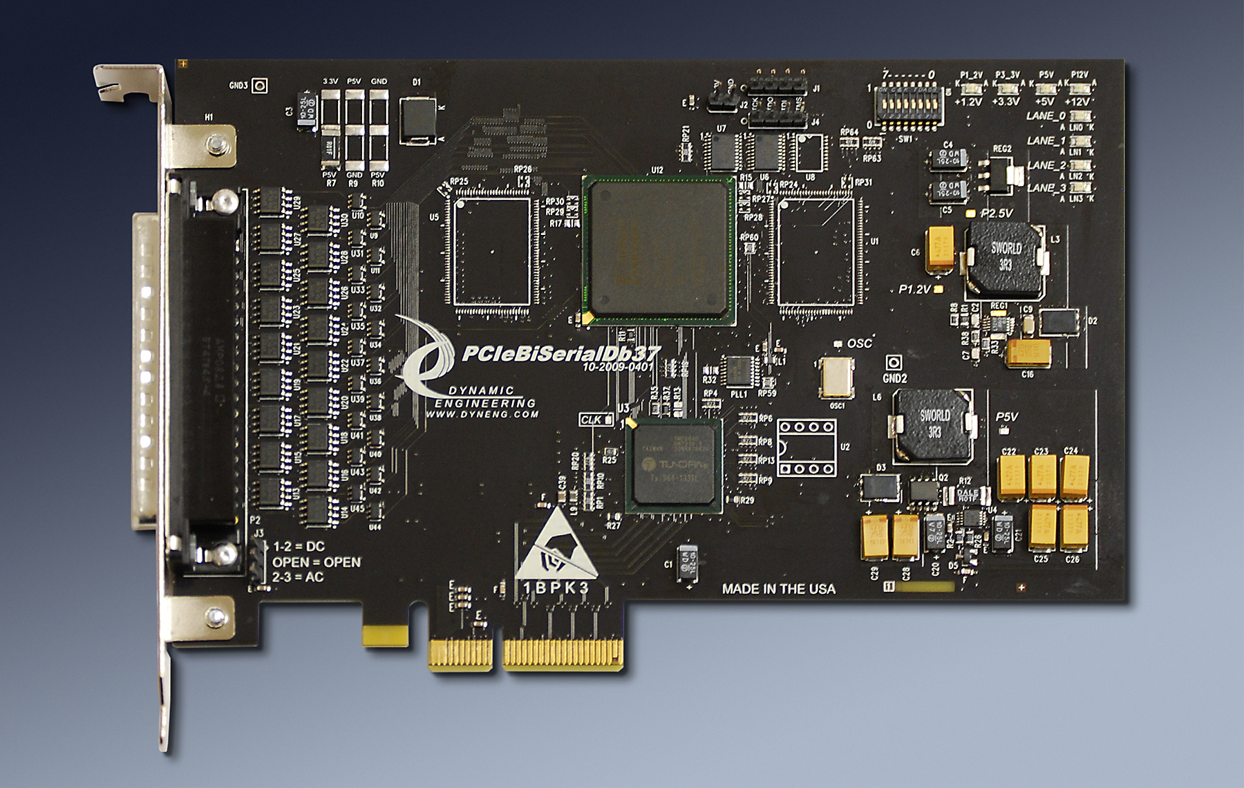
PCIe-BiSerial-DB37
PCIe Module with Spartan VI FPGA, PLL, 18 Independent Differential IO - RS422, RS-485, LVDS
Order This Item


PCIe-BiSerial-DB37 Description
- 18 independent differential IO. Each with programmable termination and direction.
- RS-485, RS-422, LVDS and mixed
- Windows, Linux
- DMA operation
- DDR 256 MBytes
- PCIe 1/2 length card with DB37 connector for IO
- Spartan 6 FPGA with BRAM for FIFO or RAM implementation
- PLL for programmable clock references (4)
- Industrial Temperature or better components
- 1 year warranty standard. Extended warranty available.
- ROHS and Standard processing available
PCIe-BiSerial-DB37 is being updated to match features with the ccPMC and PMC-BiSerial models. The main new feature is a combination of DDR and VHDL to make an easy to implement large FIFO style memory. Several designs use this buildiong block includling our SpaceWire product. 8 ports with 32 MBytes each in that case. The IO state-machines can be connected to the ports to support a variety of configuations. The [18] RS-485 / LVDS buffers have individual programmable termination, and direction controls allowing for any combination of "In´s and Out´s". Half-Duplex, Full-Duplex and uni-directional systems can be configured with software and VHDL. The FPGA is updated to a Spartan VI - 100 and the bridge interface boosted to 50 MHz.
The 18 IO can be configured to support one function, one function replicated several times, or multiple functions. For example, the "LM9" has one ARC-210 port and one GPIO port. A real space saver when you need to have some Manchester to go with your UART and HDLC ports. A partial list of functions implemented in "Channels" includes: Manchester, Miller, SDLC, UART, Serial, Parallel, GPIO, COS, Custom, LADEE, NMS, Camera, Ternary, Low Speed, High Speed, Telemetry, Master & Target interactive IO, Adaptive. To support the functions the designs include: memory elements instantiated with FIFO, Dual Port RAM, register files, as well as state-machines, counters, timers, dividers, registers, CRC and Parity generation / checking, software drivers and applications, DMA [direct memory access] and the glue that goes with it. Our designs are all written in VHDL and done in a heirarchy allowing direct porting of different features to create new implementations. Some of the design types listed are from the other BiSerial products. Due to the structure of the VHDL we frequently port or port and modify to make "just like but different " implementations.
The hardware has been used to interface with a wide variety of equipment. What do you need to communicate with? Control? Capture data from? Please see the bottom of this page and other BiSerial implementations for descriptions and manuals for our customerized versions. We have been doing custom versions of the BiSerial since 1998 when the IP version was first released.
A new custom version can be implemented in a reasonable time. Typically a few weeks design time for a medium sized project including the new VHDL set, Windows® or Linux driver, reference software package, and documentation. Examples of the designs performed to date are listed toward the bottom of this page and pages for other versions of BiSerial. Look on the models tab to see if the configuration you need already exists or if we need to work on a custom version for you.
We can be rapid with our response because the designs are structured to allow channels to be moved in and out to create new design sets. Most designs have a fairly large component of reused "known good" VHDL that we can pull from allowing us to focus on the new functions required for your implementation. You are getting the benefit of many man-years of design and test time with each new version created. Join our high reliability clients by taking advantage of our know-how to help speed your project to completion.
It all starts with the PCB [Printed Circuit Board]. Quality design and quality materials are required to meet the strenuous requirements of many of our implementations. You can do the job quickly or you can do the design correctly. We pride ourselves on taking the time to put the extra work into our layouts. The quality goes in before the parts go on. In addition to routing strategy and layer counts, Via size, plating requirements, break-out trace widths, and materials are areas where quality comes into play. The via size and method of trace attachment to the via affect the signal shape and reliability. Using tear-drop trace connections to pads, vias and through hole components enhance the reliability and minimize the impedance discontinuity resulting in a cleaner signal. Using properly sized vias provides adequate copper for proper power distribution and the surface area to bond to where traces are interconnected. The combination provides better vibration endurance than smaller vias and traces would provide. The design has several power planes with sufficient copper weight and coverage to provide the references required for the routing plus the current and voltages needed by the various devices on the board. Since 1998, when IP-BiSerial was introduced; the BiSerial family has enjoyed an excellent track record for reliability.
The PCIe interface has a published set of requirements for compliance which restrict length, impedance, loading and other factors. PCIe-BiSerial-DB37 is compliant with the PCIe Specification. The IO section has requirements based on the IO type and the purpose for the IO. A very conservative approach has been taken to allow operation with any client requirement. The IO can be LVDS or RS-485. The IO on the connector side is differential with a 100 ohm impedance requirement. Between the FPGA and the tranceivers the IO is single ended. Each IO has separate direction, termination, and data lines to allow complete flexibilty. The design has matched length connections from the FPGA ball to the seating plane of the connector. The lengths are matched to the "mil". The Impedance is controlled and the signals routed with proper spacing to avoid cross talk etc. The other features including memory, PLL, oscillator, and power supplies are implemented within the PCB to exceed the operational requirements for those devices.
Sometimes you just need more memory. With the new revision, the external FIFOs have been replaced with DDR memory. The DDR is 128Mx16. A combination of the Xilinx DDR interface and Dynamic Engineering VHDL provide a modular 32 bit high speed interface suitable for connecting to the IO ports. Each port has all of the status you would expect including the count, and programmable level based interrupts. The interface is 32 bits wide to optimize data transfer from the PCIe bus. Internal loop-back is supported. The loop-back test can be used for BIT and for software development. The programmable flags can be set to any depth to allow the software a programmable delay from event to empty or full. The interrupts can be very useful when sending or receiving messages larger than the FIFO size. The interrupts are programmable and provisions are designed to allow polling. In addition DMA can be programmed to fill or empty the FIFO with sizes larger than the FIFO size. The DMA is hardware controlled to be held off when no data is available or no room is available. With the "Channelized DMA"™ capability and large FIFOs the software application can have reduced interrupt counts while supporting larger and faster IO transfer rates.
PCIe-BiSerial-DB37 has 18 transceivers which can be used for any combination of input and output functions. Parallel and serial data, multiple channels, and different hand-shaking schemes can be implemented with the quantity of IO on PCIe-BiSerial-DB37. RS-485 transceivers support up to 50 Mhz rates. The LVDS transceivers are rated at better than 200 MHz.
The IO is available through the front panel mounted DB37 connector. Each transceiver pair is isolated from the connector with zero ohm resistors which can be replaced with alternate values should a client interface require. TVS devices protect each differential pair.
Clock options are frequently a major factor in embedded designs. Getting the right reference to the right part of the design and allowing for local control of exact frequencies. PCIe-BiSerial-DB37 has a PLL with 4 programmable outputs, reference oscillator, internal DCMs and buffering plus programable dividers instantiated within the VHDL. The PLL can be programmed to "any" fixed frequency, the DCM used to create phase variations, and local dividers to allow on-the-fly channel based frequency changes. The PLL has been updated to a Skyworks Solutions model with built in extremely stable reference, plus differential outputs to provide a higher bandwidth solution with lower noise on-board [LVDS levels]. The differential pairs are received and terminated within the FPGA.
"Channelized DMA"™ is an important feature of the PCIe-BiSerial-DB37 design. With "Channelized DMA"™ you have a separate DMA engine for each transmitter and receiver port within each channel. Each state-machine can be serviced independently with DMA without requiring intervention from the host. Large data transfers can happen between multiple connections while the CPU is off doing something else. In non-channelized designs the CPU will have to intervene each time a different port needs to be serviced. With a channelized approach the hardware takes care of the local arbitration, and eliminates the intervention for better system performance and less latency.
If your situation demands a custom application we will update the Xilinx FPGA and IO components. Send us your timing and we will send you the interface. Please refer to the bottom of this page for previously completed "customerized" PCIe-BiSerial-DB37 implementations.
email us your wish list or call today
PCIe-BiSerial-DB37 Example Block Diagram
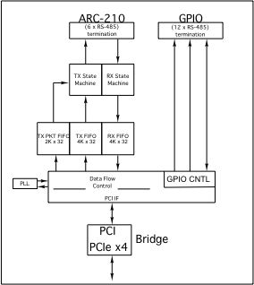
PCIe-BiSerial-DB37 LM9 (ARC-210) version block diagram
The 18 IO can be configured to support one function, one function replicated several times, or multiple functions. For example, the "LM9" has one ARC-210 port and one GPIO port. A real space saver when you need to have some Manchester to go with your UART and HDLC ports. A partial list of functions implemented in "Channels" includes: Manchester, Miller, SDLC, UART, Serial, Parallel, GPIO, COS, Custom, LADEE, NMS, Camera, Ternary, Low Speed, High Speed, Telemetry, Master & Target interactive IO, Adaptive. To support the functions the designs include: memory elements instantiated with FIFO, Dual Port RAM, register files, as well as state-machines, counters, timers, dividers, registers, CRC and Parity generation / checking, software drivers and applications, DMA [direct memory access] and the glue that goes with it. Our designs are all written in VHDL and done in a heirarchy allowing direct porting of different features to create new implementations. Some of the design types listed are from the other BiSerial products. Due to the structure of the VHDL we frequently port or port and modify to make "just like but different " implementations.
The hardware has been used to interface with a wide variety of equipment. What do you need to communicate with? Control? Capture data from? Please see the bottom of this page and other BiSerial implementations for descriptions and manuals for our customerized versions. We have been doing custom versions of the BiSerial since 1998 when the IP version was first released.
A new custom version can be implemented in a reasonable time. Typically a few weeks design time for a medium sized project including the new VHDL set, Windows® or Linux driver, reference software package, and documentation. Examples of the designs performed to date are listed toward the bottom of this page and pages for other versions of BiSerial. Look on the models tab to see if the configuration you need already exists or if we need to work on a custom version for you.
We can be rapid with our response because the designs are structured to allow channels to be moved in and out to create new design sets. Most designs have a fairly large component of reused "known good" VHDL that we can pull from allowing us to focus on the new functions required for your implementation. You are getting the benefit of many man-years of design and test time with each new version created. Join our high reliability clients by taking advantage of our know-how to help speed your project to completion.
It all starts with the PCB [Printed Circuit Board]. Quality design and quality materials are required to meet the strenuous requirements of many of our implementations. You can do the job quickly or you can do the design correctly. We pride ourselves on taking the time to put the extra work into our layouts. The quality goes in before the parts go on. In addition to routing strategy and layer counts, Via size, plating requirements, break-out trace widths, and materials are areas where quality comes into play. The via size and method of trace attachment to the via affect the signal shape and reliability. Using tear-drop trace connections to pads, vias and through hole components enhance the reliability and minimize the impedance discontinuity resulting in a cleaner signal. Using properly sized vias provides adequate copper for proper power distribution and the surface area to bond to where traces are interconnected. The combination provides better vibration endurance than smaller vias and traces would provide. The design has several power planes with sufficient copper weight and coverage to provide the references required for the routing plus the current and voltages needed by the various devices on the board. Since 1998, when IP-BiSerial was introduced; the BiSerial family has enjoyed an excellent track record for reliability.
The PCIe interface has a published set of requirements for compliance which restrict length, impedance, loading and other factors. PCIe-BiSerial-DB37 is compliant with the PCIe Specification. The IO section has requirements based on the IO type and the purpose for the IO. A very conservative approach has been taken to allow operation with any client requirement. The IO can be LVDS or RS-485. The IO on the connector side is differential with a 100 ohm impedance requirement. Between the FPGA and the tranceivers the IO is single ended. Each IO has separate direction, termination, and data lines to allow complete flexibilty. The design has matched length connections from the FPGA ball to the seating plane of the connector. The lengths are matched to the "mil". The Impedance is controlled and the signals routed with proper spacing to avoid cross talk etc. The other features including memory, PLL, oscillator, and power supplies are implemented within the PCB to exceed the operational requirements for those devices.
Sometimes you just need more memory. With the new revision, the external FIFOs have been replaced with DDR memory. The DDR is 128Mx16. A combination of the Xilinx DDR interface and Dynamic Engineering VHDL provide a modular 32 bit high speed interface suitable for connecting to the IO ports. Each port has all of the status you would expect including the count, and programmable level based interrupts. The interface is 32 bits wide to optimize data transfer from the PCIe bus. Internal loop-back is supported. The loop-back test can be used for BIT and for software development. The programmable flags can be set to any depth to allow the software a programmable delay from event to empty or full. The interrupts can be very useful when sending or receiving messages larger than the FIFO size. The interrupts are programmable and provisions are designed to allow polling. In addition DMA can be programmed to fill or empty the FIFO with sizes larger than the FIFO size. The DMA is hardware controlled to be held off when no data is available or no room is available. With the "Channelized DMA"™ capability and large FIFOs the software application can have reduced interrupt counts while supporting larger and faster IO transfer rates.
PCIe-BiSerial-DB37 has 18 transceivers which can be used for any combination of input and output functions. Parallel and serial data, multiple channels, and different hand-shaking schemes can be implemented with the quantity of IO on PCIe-BiSerial-DB37. RS-485 transceivers support up to 50 Mhz rates. The LVDS transceivers are rated at better than 200 MHz.
The IO is available through the front panel mounted DB37 connector. Each transceiver pair is isolated from the connector with zero ohm resistors which can be replaced with alternate values should a client interface require. TVS devices protect each differential pair.
Clock options are frequently a major factor in embedded designs. Getting the right reference to the right part of the design and allowing for local control of exact frequencies. PCIe-BiSerial-DB37 has a PLL with 4 programmable outputs, reference oscillator, internal DCMs and buffering plus programable dividers instantiated within the VHDL. The PLL can be programmed to "any" fixed frequency, the DCM used to create phase variations, and local dividers to allow on-the-fly channel based frequency changes. The PLL has been updated to a Skyworks Solutions model with built in extremely stable reference, plus differential outputs to provide a higher bandwidth solution with lower noise on-board [LVDS levels]. The differential pairs are received and terminated within the FPGA.
"Channelized DMA"™ is an important feature of the PCIe-BiSerial-DB37 design. With "Channelized DMA"™ you have a separate DMA engine for each transmitter and receiver port within each channel. Each state-machine can be serviced independently with DMA without requiring intervention from the host. Large data transfers can happen between multiple connections while the CPU is off doing something else. In non-channelized designs the CPU will have to intervene each time a different port needs to be serviced. With a channelized approach the hardware takes care of the local arbitration, and eliminates the intervention for better system performance and less latency.
If your situation demands a custom application we will update the Xilinx FPGA and IO components. Send us your timing and we will send you the interface. Please refer to the bottom of this page for previously completed "customerized" PCIe-BiSerial-DB37 implementations.
email us your wish list or call today

PCIe-BiSerial-DB37 LM9 (ARC-210) version block diagram
PCIe-BiSerial-DB37 Features
Size
1/2 length PCIe - max dimensions including gold fingers 6.6" x 4.375"
IO
IO is available on a DB37 connector via PCIe bezel. The differential IO is properly routed with impedance control, pitch, and space plus matched lengths across all of the pairs. Up to 50 MHz with RS-485, and up to 200 MHz with LVDS IO types.
Clocks
4 lane PCIe Gen1, 50 MHz oscillator ( other frequencies available), 4 programmable PLL inputs, Counters / Dividers / DCM for local clock control.
Interface Types
Custom programmed interfaces are available. Please send us a timing diagram, and we can program one for you. Most interfaces can be adapted from our large library of designs within a few weeks including the updated VHDL, Windows or Linux Driver, reference manuals etc. We can support on-site [ours] integration to help you get your application level software working.
Alternatively choose one of the already completed versions and purchase off-the-shelf. Common requested and implemented interface types include: Manchester, Miller, SDLC, UART, Serial, Parallel, GPIO, COS, Custom, LADEE, NMS, Camera, Ternary, Low Speed, High Speed, Telemetry, Master & Target interactive IO, Adaptive. Mix and Match. Just like but different...
Alternatively choose one of the already completed versions and purchase off-the-shelf. Common requested and implemented interface types include: Manchester, Miller, SDLC, UART, Serial, Parallel, GPIO, COS, Custom, LADEE, NMS, Camera, Ternary, Low Speed, High Speed, Telemetry, Master & Target interactive IO, Adaptive. Mix and Match. Just like but different...
Memory
Spartan VI - 100 is standard and has BRAM to create RAM, FIFO etc., 256 MBytes DDR attached to FPGA
Software Interface
Control registers are read-writeable
Windows®, Linux reference SW and Drivers
Windows®, Linux reference SW and Drivers
Interrupts
Software programmable interrupts on status, errors, completion of transfer, DMA, FIFO levels, custom events. Status can be polled for non-interrupt driven operation as well.
Power Requirement
+12 and 3.3V from PCIe connector. Local 2.5V, 1.8V, 1.2V converted with on-board power supplies. No power cables are required for this design.
LEDs
6 provided as indicators for Power Good, DDR clock locked.
Volatility
Reliability
TBD million hours. Bellcore. GB 25c
PCIe-BiSerial-DB37 Benefits
Speed
PCIe-BiSerial-DB37 can offload your CPU and increase system speed. The IO rate is high enough to support many protocols allowing for system upgrades, replacement of older boards, and relocating processes done in SW to the HW as needed.
Price
System level cost is best when reasonably priced reliable hardware is used and NRE minimized. With PCIe-BiSerial-DB37, driver support, reference software, history of reliable operation, and fantastic client support your cost per unit and overall costs are attractive.
Ease of Use
PCIe-BiSerial-DB37 is designed to be easy to use. Direct access to all features, aligned registers for larger access types, programmable features to allow personalization for your system. Please download the manuals and see for yourself. Reference software is provided in source form to get you started.
Availability
There are two basic models with LVDS or RS-485 IO types. Built to order with our in-house manufacturing capability allowing for quick delivery. New NRE required designs will have some delay to implement, integrate and test.
PCIe Specification Compatibility
PCIe-BiSerial-DB37 is compliant per the PCI-SIG specifications.
Part Number: PCIe-BiSerial-DB37
Ordering Options
- PCIe-BiSerial-DB37 Standard board - with RS485 IO
- -LVDS Switch to LVDS IO
- -ROHS Use ROHS processing. Standard processing is ""leaded"
- -CC Option to add Conformal Coating
- -XXX See Models section for customized versions and replace XXX with type "-LM9" for example
PCIe-BiSerial-DB37 Drivers
Software Support for PCIe-BiSerial-DB37-XXX includes: Windows®, and Linux compliant drivers
Please see the Driver manuals for the specifics of each type.
Drivers and Reference SW are developed for each type / version of PCIe-BiSerial-DB37 implemented. When custom versions are ordered the NRE will include providing Windows, Linux, and or VxWorks packages. For off-the-shelf models, select on the manuals tab, the Windows® and Linux SW shown is included with your purchase of the HW. A small one-time charge is required for the VxWorks versions. Unsupported SW versions may have an NRE requirement.
Integration support is available. Please contact Dynamic Engineering for this option or download the Technical Support Description from the Company button.
PCIe-BiSerial-DB37 Models
PCIeBiSerialDb37 version ARC-210 AKA LM9
Client: Lockheed Martin
The LM9 protocol provides an ARC-210 compatible interface plus a GPIO port. The main purpose is to allow data communications using the ARC-210. The ARC-210 interface is bidirectional and is fully independent for Tx and Rx. Each side is supported with 4Kx32 Data FIFO plus 2Kx32 Packet FIFO. The transmitter "SendTiming" signal can be set to output the reference clock to allow for loop-back and alternate purpose uses. Interrupt or polled operation. "Channelized DMA"™ on TX and RX. 12 bit GPIO port [termination, direction independent on each bit]. RS-485 IO. TX in transmit SendTiming mode supported with PLL for user frequency.

LM9 simplified transmit timing diagram
Download the LM9 - ARC-210 interface Hardware manual
Download the LM9 Windows® manual
Download the LM9 - ARC-210 Windows 10® manual
Download the LM9 Linux manual
PCIeBiSerialDb37 version RTN8
Client: restricted
The RTN8 protocol implemented provides an 8 bit parallel port and reference clock. LVDS IO definition. Programmable TX rate using on-board PLL. Autobauding RX port. 12Kx32 Tx FIFO buffer. 256K+x32 RX buffer. Interrupt or polled operation. "Channelized DMA"™ on TX and RX.

RTN8 simplified transmit timing diagram
Download the RTN8 Hardware manual
Download the RTN8 Linux manual
PCIeBiSerialDb37 version BA22
Client: Boeing
The BA22 protocol implemented provides a 2 bit serial transfer with clock and Sync. Transmit and Receive funtions. LVDS IO definition. Programmable TX rate using on-board PLL. Autobauding RX port. ~262K x32 Tx FIFO buffer. 5Kx32 RX buffer. Interrupt or polled operation. "Channelized DMA"™ on TX and RX. Image format data with: Programmable line length, idles between lines, frame length, PreAmble and Sync. Control characters for all four phases are programmable.

BA22 simplified transmit timing diagram
Download the BA22 Hardware manual
PCIeBiSerialDb37 version L3Com1
Client: L3
L3Com1 is an update to the RTN8 design to include a flow control signal and to add packet control options. Operates as 1/2 duplex with LVDS IO. L3Com1 protocol implemented provides an 8 bit parallel port, reference clock, Valid, and BackPressure signals. Programmable TX rate using on-board PLL. Autobauding RX port. 12Kx32 Tx FIFO buffer. 262Kx32 RX buffer. Packetized with byte count programmability. Interrupt or polled operation. "Channelized DMA"™
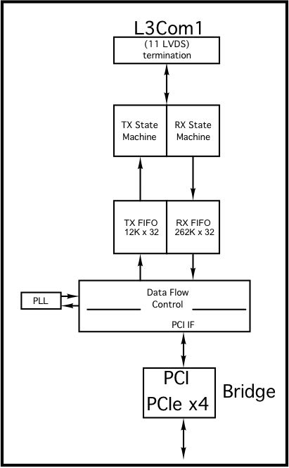
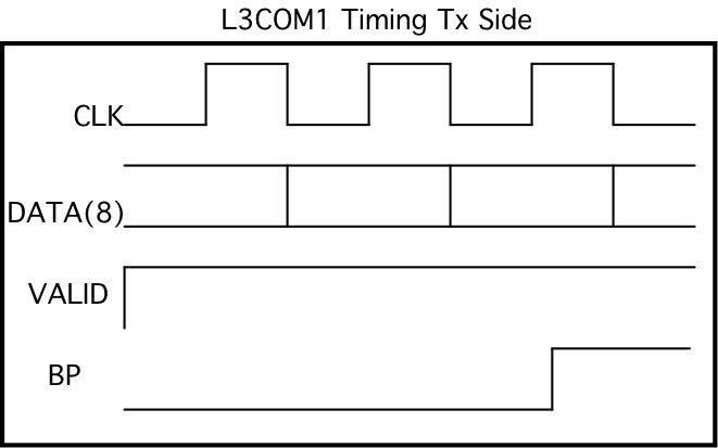
L3COM1 simplified Block and transmit timing diagrams
Download the L3Com1 Hardware manual
Download the L3Com1 Linux manual
Windows 10 support package is in development. Linux drivers and Windows 7 basic driver available now.
Client: Lockheed Martin
The LM9 protocol provides an ARC-210 compatible interface plus a GPIO port. The main purpose is to allow data communications using the ARC-210. The ARC-210 interface is bidirectional and is fully independent for Tx and Rx. Each side is supported with 4Kx32 Data FIFO plus 2Kx32 Packet FIFO. The transmitter "SendTiming" signal can be set to output the reference clock to allow for loop-back and alternate purpose uses. Interrupt or polled operation. "Channelized DMA"™ on TX and RX. 12 bit GPIO port [termination, direction independent on each bit]. RS-485 IO. TX in transmit SendTiming mode supported with PLL for user frequency.

LM9 simplified transmit timing diagram
Download the LM9 - ARC-210 interface Hardware manual
Download the LM9 Windows® manual
Download the LM9 - ARC-210 Windows 10® manual
Download the LM9 Linux manual
PCIeBiSerialDb37 version RTN8
Client: restricted
The RTN8 protocol implemented provides an 8 bit parallel port and reference clock. LVDS IO definition. Programmable TX rate using on-board PLL. Autobauding RX port. 12Kx32 Tx FIFO buffer. 256K+x32 RX buffer. Interrupt or polled operation. "Channelized DMA"™ on TX and RX.

RTN8 simplified transmit timing diagram
Download the RTN8 Hardware manual
Download the RTN8 Linux manual
PCIeBiSerialDb37 version BA22
Client: Boeing
The BA22 protocol implemented provides a 2 bit serial transfer with clock and Sync. Transmit and Receive funtions. LVDS IO definition. Programmable TX rate using on-board PLL. Autobauding RX port. ~262K x32 Tx FIFO buffer. 5Kx32 RX buffer. Interrupt or polled operation. "Channelized DMA"™ on TX and RX. Image format data with: Programmable line length, idles between lines, frame length, PreAmble and Sync. Control characters for all four phases are programmable.

BA22 simplified transmit timing diagram
Download the BA22 Hardware manual
PCIeBiSerialDb37 version L3Com1
Client: L3
L3Com1 is an update to the RTN8 design to include a flow control signal and to add packet control options. Operates as 1/2 duplex with LVDS IO. L3Com1 protocol implemented provides an 8 bit parallel port, reference clock, Valid, and BackPressure signals. Programmable TX rate using on-board PLL. Autobauding RX port. 12Kx32 Tx FIFO buffer. 262Kx32 RX buffer. Packetized with byte count programmability. Interrupt or polled operation. "Channelized DMA"™


L3COM1 simplified Block and transmit timing diagrams
Download the L3Com1 Hardware manual
Download the L3Com1 Linux manual
Windows 10 support package is in development. Linux drivers and Windows 7 basic driver available now.

